Sign up for our newsletter!
Your data will be handled in compliance with our privacy policy.
Your data will be handled in compliance with our privacy policy.

Research paper published in Solid–State Electronics, Volume 139, January 2018, pp. 75–79.
A M Saleem, R Andersson, V Desmaris, P Enoksson • October 16, 2017
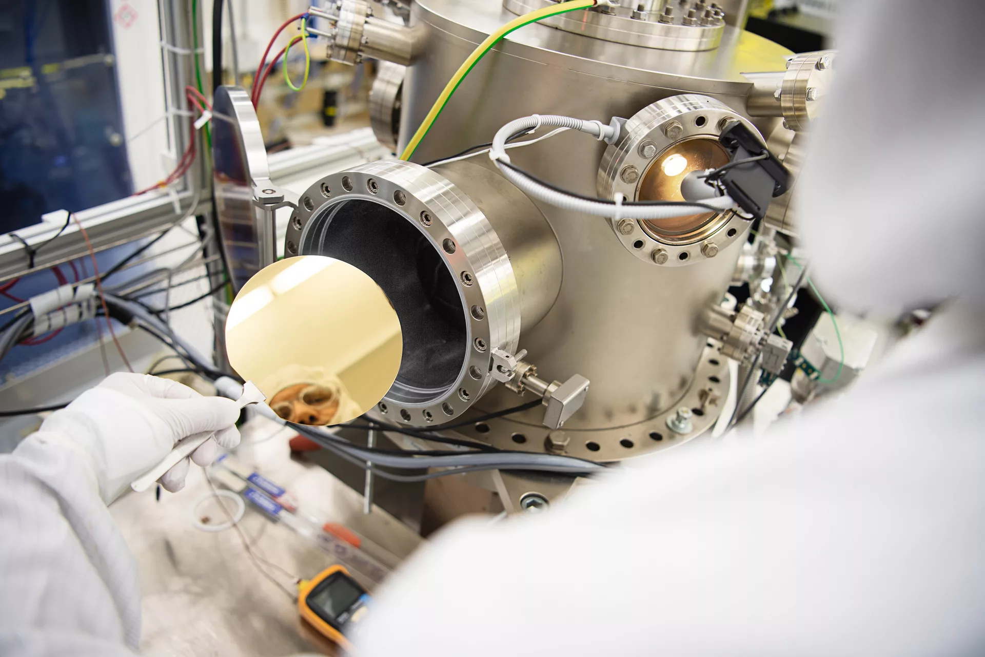
Complete miniaturized on-chip integrated solid-state capacitors have been fabricated based on conformal coating of vertically aligned carbon nanofibers (VACNFs), using a CMOS temperature compatible microfabrication processes. The 5 µm long VACNFs, operating as electrode, are grown on a silicon substrate and conformally coated by aluminum oxide dielectric using atomic layer deposition (ALD) technique. The areal (footprint) capacitance density value of 11–15 nF/mm2 is realized with high reproducibility. The CMOS temperature compatible microfabrication, ultra-low profile (less than 7 µm thickness) and high capacitance density would enables direct integration of micro energy storage devices on the active CMOS chip, multi-chip package and passives on silicon or glass interposer. A model is developed to calculate the surface area of VACNFs and the effective capacitance from the devices. It is thereby shown that 71 % of surface area of the VACNFs has contributed to the measured capacitance, and by using the entire area the capacitance can potentially be increased.
Your data will be handled in compliance with our privacy policy.