Sign up for our newsletter!
Your data will be handled in compliance with our privacy policy.
Your data will be handled in compliance with our privacy policy.

Research paper in the proceedings of 2nd International Conference on Materials for Energy (EnMat II), Karlsruhe, Germany, 12–16 May, 2013.
H Staaf, A M Saleem, G Göransson, P Lundgren, P Enoksson • May 12, 2013
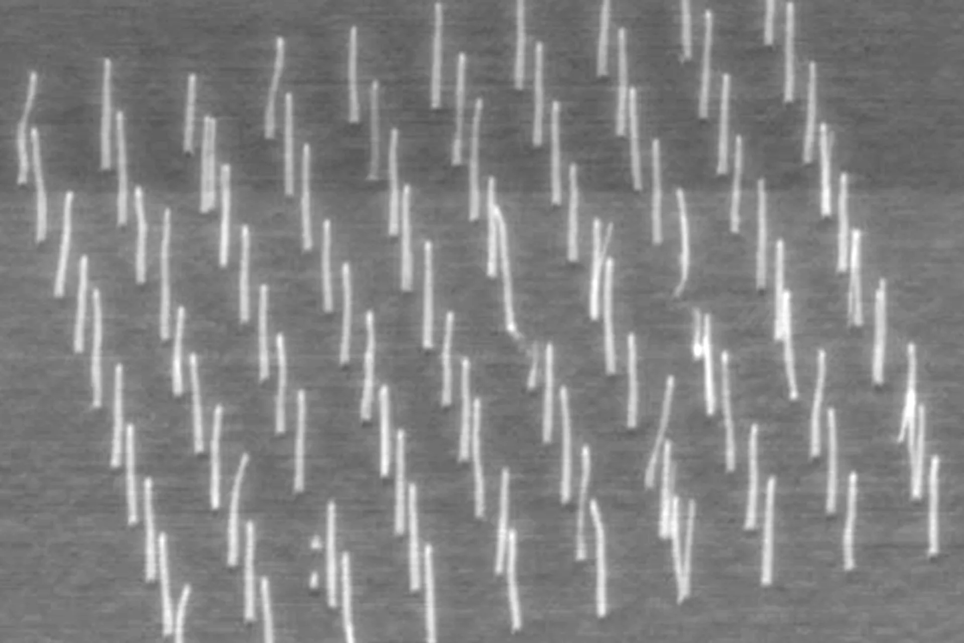
One-dimensional carbon nanostructures have been known and fabricated for more than a hundred years and were originally rWe describe a fast and cost-effective process for the growth of carbon nanofibers (CNFs) at a temperature compatible with Both silicon wafers and thermally oxidized silicon wafers are diced into 14×14 mm2 pieces to fit the circular active area with 11 mm diameter used in voltammetry. 50 nm of tungsten is sputtered on both sides of the chips for edge coverage to have better electrical contact of back side and grown side. A catalyst layer consisting of aluminum (5 nm) and iron (2 nm) is deposited using electron beam evaporation. The CNTs are grown by chemical vapor deposition at 700 °C using acetylene and hydrogen gasses as carbon source and carrier. First, the catalyst is pretreated at 500 °C in the environment of continuous hydrogen flow at around 8 mbar pressure. Then acetylene is introduced and the temperature is raised to 700 °C within a few seconds. Sample (1) consists of: Si, W, Al, Fe; sample (2) consists of: Si, SiO2, W, Al, Fe. Measurements were carried out by a three electrode system with Ag/AgCl as reference electrode, Pt as counter electrode and 1M KOH as electrolyte. The capacitance was calculated from the voltammogram (Figure 1). The voltammetry was carried out with 5 cycles per sample. Sample (1) yields a capacitance of 0.0475 F and (2) a apacitance of 0.04 F for the active geometrical surface at sweep rate 20 mV/s (Table 1). Calculated capacitances are from the voltammogram values, where the capacitance is the absolute value between ‑0.1 – 0.1 V divided by 2 and divided by the sweep rate. C = Δ|I| / s, where Δ|I| is the difference in current, s is the sweep rate (dE/dt) and C is the capacitance. An estimation of CNT weight using SEM pictures yields approximately 0,3 mg. The measured weight from a scale is in the range 0.8–1.4 mg which gives a specific capacitance of 13P1: 46.9 ± 12.7 F/g and 14P1: 39.3 ± 10.7 F/g for the two samples respectively. Future improvements of these CNT electrodes will be to produce longer nanotubes and a more dense structure. Both these parameters will increase the surface area and by that yield a higher capacitance for the electrode. By con-trolling the vertical alignment of the CNTs in combination with production methods containing cheap materials and by using industrial fabrication techniques the energy density can be improved. This makes vertically aligned CNT a very promising material as electrode material for supercapacitors.
Your data will be handled in compliance with our privacy policy.