Sign up for our newsletter!
Your data will be handled in compliance with our privacy policy.
Your data will be handled in compliance with our privacy policy.

Research paper in the proceedings of NT11 International Conference on the Science and Application of Nanotubes, University of Cambridge, United Kingdom, July 10–16, 2011.
V Desmaris, A M Saleem, J Berg, P Enoksson, S Kabir, L-G Huss, R Jonsson, S Rudner, M Höijer, A Tamburrano, M S Sarto • July 10, 2011
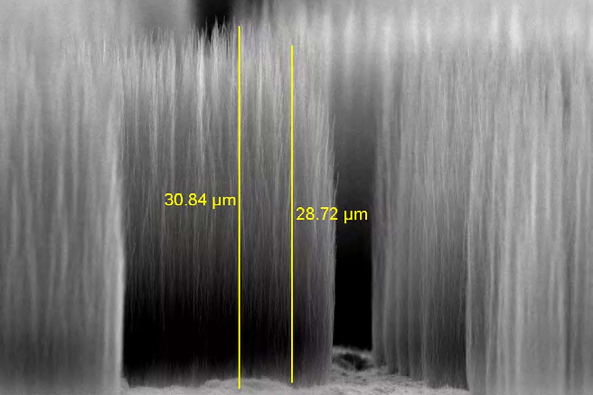
We have developed an RF test vehicle suitable for measuring DC and microwave performance of vertically grown carbon nanostructures (VGCNS) as via-interconnects. A first version of the interconnect test vehicles devices were designed, fabricated and characterized. The RF small signal (S‑parameter) and large signal measurements show that carbon nanofibres can be used as interconnects in microwave circuit, even for power devices. The design of test vehicle employs a three metal layer concept, forming sequentially the ground, signal and device under test structures for characterization in a microstrip configuration. The structures as such consisted of interconnects of dimensions ranging from 50 nm to 100 µm diameter made of VGCNS. In the first version of the interconnect test vehicles, the interconnects were made of carbon nanofibers grown at 450 C. From SEM measurement we found that the resulting height was around 1.5–2 µm. Epoxy polymer SU‑8 was employed by spinning on the device and a subsequent etch back process was carried out to open up the tip of the fibres to connect to consecutive interconnects with the third metallisation layer. After growing the nanofibres, it was observed, using SEM, that interconnect sizes smaller than 10 µm diameter suffered from parasitic growth and therefore the effective device dimension deviated from the initial design. We carried out small signal measurements using a vector network analyser for frequency ranging from 1 to 25 GHz, in order to characterise the transmission and reflection/absorption of the devices as function of their diameter size. The large signal evaluation was performed by measuring the gain compression of the devices. In addition destructive tests, aiming at testing the current carrying capability of the interconnect, have also been performed. The resistivity of interconnects was measured to vary varies from 0.2–1.3 mΩ·mm. Apparently, the device performance is considerably influenced by the fill factor of the interconnect with VGCNS. Small variations in fill factor (in %) provided a large variations in device resistivity. Furthermore, it was also observed that the resistance drops at higher power levels. RF conductivity of interconnects ranges from 5×10³ S/m to 7×10⁵ S/m. The average input power before interconnect destruction is larger than 25W with effective device diameter ranging from 3 µm to 100 µm interconnects. In addition, the average gain compression before interconnect destruction was found to be 0.6 dB. It was not possible to extract the conductivity value of an individual nanofiber using comparison to simulation data, since the devices might have suffered from parasitic growth as well as pinhole metal diffusion during top metal contact formation. This certainly affects the actual device dimension and properties. Nevertheless, the proof of concept of design and manufacturing a test vehicle for RF measurements of vertically grown nanostructures was achieved. We will report the findings and anomalies in the measured devices. Further improvement is expected in the coming test vehicle version.
Your data will be handled in compliance with our privacy policy.